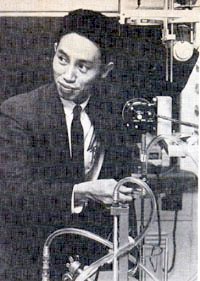
10.3.1.3 - THE TUNNEL DIODE
Originally, an extremely abrupt junction between very highly doped P and N regions of a Gemanium matrix, to make the depletion regions of the diode very thin, on the order of a few hundreds of Angstrons, formed such semiconductor device. In effect due to its behavior to a negative resitance, the Tunnel diode could be put to use for high-frequency amplification, oscillation or switching. Due to its high speed in signal processing, around 100 picoseconds, manufactures foresaw many applications for such a kind of device. Fig 256 Therefore the interest in the tunnel diode waned rapidly due to the improvement in the Transistor technology as well as the birth of the integrated circuit, which was the fundamental element for the manufacturing of computer memory, originally the purpose of the device invented by Dr. Esaki. Gaining in importance throughout the late fifities and early sixties were semiconductor devices whose operation extended to the uppermost frequency and beyond to the visible-light spectrum. Most of these emerged from compound semiconductors such as Gallium Arsenide and Indium Phosphide, which led to the invention of light emitting diode |