10.3 - FROM THE DIODE TO THE TRANSISTOR
THE MAN-MADE CRYSTAL
THE MAN-MADE CRYSTAL
Through the researches
in the new field of solid state Physics scientists discovered that
the atomic structure of certain materials like Germanium and Silicon,
contains few free electrons that could scape leaving holes of vacancies
of charges in the crystal lattice.
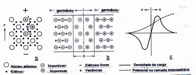
Basically, this kind of man-made diode consists in handling the Germanium atomic structure by adding into its crystal lattice small quantities of impurities known as DOPE. Those impurities are atoms of several chemical elements, generally metals comprising their own electronic configuration. For instance, Phosphor, Arsenium and Antimony have 5 electrons in their outer orbit while Aluminium, Indium and Galium or Boron only 3.
When adding those impurities into the Germanium crystal lattice, two kinds of crystalline structure are formed: amixture containing surplus of free electrons, also called NEGATIVE GERMANIUM; another one with shortage of electrons known as POSITIVE GERMANIUM. By joinning together a P and N Germanium, an electrical charge transfer occurs at the boundary layer of the P-N junction. Thus, P and N crystals have a surplus and shortage of electrons respectively. Those charges repel each other preventing further diffusion of electons and holes in the
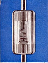
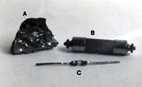
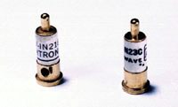
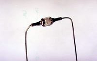
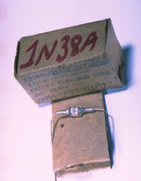
In principle the first point contact diode was almost identical to that earliest types of crystal detectors. Basically it comprises a pellet of Germanium with a flat polished surface was where it was soldered soldered to one of the connecting wires; the other wire is provided with a sharply point springy Tungsten end, similar to the cat'whisker principle invented by Pickard. Fig 249 The Germanium diode had several advantages when compared with the diode valve such as: no heater, low cost, small volume and it could operate either as a detection as well as a switching device. In the beguinning its main application was in the manufacturing of televisers and computers. Fig 250 As aforementined, the point-contact diodes were an improved version of the original crystal detector. Fig 251 In this way, soon they were replaced by whiskerless diodes whose operational principle was related with the uniform thickness configuration of the junctions in the semi-conductor material.
|