|
The search for a
reliable solid-state amplifier was envisioned earlier around 1920.
It is interesting to note that more common attempts were based on
the field-effect principle, most likely because its concept was
akin to the grid-control action of the thermionic valves, i.e. crystal
device controlled by voltage instead of current.
In 1920, based in his pioneering researches the German physicist
working in the USA, Julius E. Lilienfeld managed to obtein several
patents for an amplifier design based on Copper Sulfide.
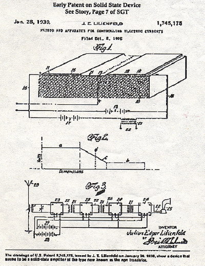 |
Reproduction of the patent
nº 1,745,175, granted to the physicist J.E. Lilienfeld
by the US Patent Office in January 1930, describing an early
method and a solid-state apparates for controlling electric
current later on invented by Bell Laboratories under the name
of transistor.
|
However, since his experiments were conducted in near obscurity
he was unable to draw serious attention to it. Around 1935 in England,
one of the first patents was issued to the German inventor Oscar
Heil for a field -effect crystal amplifier.
Basically its concept used a control electrode to regulate the current
flow through a thin semiconductor layer made with several types
of materials like Copper Oxide, Vanadium Pentoxide, Tellurium and
Iodine. In reality the Heil proposal for such a kind of crystal
amplifier was the forerunner of the insulated-gate field effect
transistor, since the control electrode was isolated from the semiconductor
substrate.
In later thirties, early researches in photoelectricity started
by the german physicist R.W. Pohl gave birth to a slow-acting triode
relied on a wire grid to control the flow of elctrons through a
heated Potassium Bromide crystal.
Even considering it was just a laboratory work nonetheless it proved
its theoretical feasibility to obtain signal amplification through
a field-effect solid-state device.
As aforeseen, the researches to obtain the first solid-state amplifier
operating by the field-effect principle used modulation current
flowing through a chunck of semiconductor material by injection
of chargers carriers through a gate or grid, which should be isolated
from the slab.
However, the injected charge carriers should not affect the flow
of current through the semiconductor slab because they got trapped
in the material's surface. It is interesting to note that although
the simplicity of the field-effect solid-state amplifier's operating
concept, due to the misundersanding of the behavior of the layer
formation, later explained by Bardeen, through his "theory
of surface state", its practical development was destine to
come only after the invention of a far complex semiconductor device,
the bipolar transitor.
In the later fifties semiconductor associated industries had a substantialy
expanse of the business. The perenial saga for technically improve,
high performance and affordable cost semiconductor devices led the
engineers to revive the field-effect transitor researches considering
mainly its simple concept and low operation consumption.
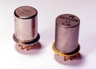 |
| To the left " FETRON"
manufactured by" Teledyne" ; right the HIN or "
Hybrid Integrated Network" , to left the " FETRON"
a solid state component, however manufactured for " Western
Electric". |
In 1958, Stanislas Teszner, a polish scientist, working for a
subsidiary of General Electric in France finally developed the first
field-effect transistor without an isulated gate, made in Germanium
alloy for operation in high frequency range and sold under the trade
name of TECNITRON.
In the USA the company Teledyne made the first junction field-effect
transitor in 1960. Later in 1967, the company launched in the market
an interesting linear semiconductor system using this type of transitor
that was sold under the tradename of FETRON.
In reality the FETRON comprised a set of junction-field-effect device
cascode-connected. It was orginally developed to replace the enormous
quantities of thermionic valves type pentodes and tetrodes used
in the American telephone system due to their several operational
disadvantages when compared with TRANSISTORS.
It can be seen that the first types junction-field-effect devices
used the depletion region of a reverse-biased pn junction to control
the effective cross section and so the condutivity of a crystal
substrate.
Working together in the researche laboratories of RCA, Steve Hofstein
and Frederic Heiman, using the new and updated Planar technology
developed by Fairchild, they introduced a modification in the configuration
of the junction-field-effect transistor.
Thus, a metal gate, insulated from the Silicon material by a layer
of Silicon Oxide, replaced the reverse-biased junction control structure
of the junction-field-effect transistor.
Finally the engineers succceded in building a reliable field-effect
transitor with insulated gate according to the original concept
proposed by Heil in 1935, giving birth to the MOSFET semiconductor,
an acronym for metal-oxide-semiconductor field-effect transitor.
The MOS technology was a big step in the semiconductor manufacturing
as through the same it was possible to build in a very small area
in the crystal matrix several types of components like diodes, transistors,
led to the new field of the microelectronics. |