The behavior of electrons
in solids were quantified by Erwin Shchrodinger's famous quantum-mechanical
equation in 1926.While the theoretician were unraveling the concepts
of electrons, band theories, and valences, practical mind oriented
scientists like: Mevil F. Mott in England, Alexander Davidov in Russia
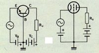 |
| Grounded base or grounded grid circuit compared
with a grounded grid in a triode valve. |
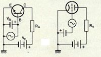 |
| Grounded emitter or grounded cathode circuit
compared with a grounded cathode in a triode valve. |
and as aforementioned Walter Schottky in Germany, were experimenting
with various types of crystals to explain metal-semiconductor rectification.
The rectification mechanism was generally agreed upon: the semiconductor
material becomes depleted of current carriers at the junction, which
creates an effective barrier to equilibrium electron flow across
the junction. Application of an electric field that reduces the
barrier allows electron flow, while reversal of that field further
deplets the semiconductor carriers, thus heightening the barrier
to electron flow.
As aforeseen over many years, since the end of XIX century, the
search for a reliable solid-state amplification device was the saga
of many scientists' engineers and inventors.
Therefore it happened only in 1948 when a team of physicists, William
Shcockley, John Bardeen and Walter
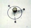 |
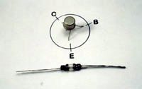
| Close up view of the solid-state amplifer
showing its three contacts points: EMITTER (E), COLLECTOR (C),
and BASE (B). |
H. Brattain, working at Bell Laboratories, USA, established on
a theorical basis that in
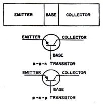 |
| Diagram describing the reversal polarities
of the TRANSISTORS N-P-N and P-N-P. |
such semiconducting device the flow of a acurrent sent through
the two contacts could be controlled by means of a current sent
by a third contact similar to the grid behavior found in a thermionic
valve or tiode. Fig 259
This device was christenned as TRANSISTOR, an acronym for: TRANSFER
AND RESISTOR. Fig 260
In terms of an electrical circuit, the TRANSISTOR is a set of two
diodes operating in opposition to each other, the N-P-N crystalline
strucuture of which is provided with three contact points or electrodes
denominated: EMITTER and COLLECTOR which are connected to the two
N crystals, while a third one or BASE is connected to the positive
portion or P crystal. Fig 261
 |
| The TRANSISTOR or semiconductor device provide
with three contact points compared with an early Germanium diode
|
This semiconducting device is also called bipolar TRANSISTOR.
In its normal operation, the emitter to base junction is biased
in the forward direction and the collector to base function in the
reverse direction. Fig 262
Both types, N-P-N and P-N-P TRANSISTORS operate identically. However,
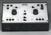 |
| TRANSISTOR curve tracer showing in its front
panel the polarity reversal switch for testing P-N-P and N-P-N
TRANSISTORS. |
considering those two kinds of crystalline structurer, they have
reverse polarities. Fig 263 Thus, while in the N-P-N the electrons
flow from the emitter to the collector, in the P-N-P they flow from
the collector to the emitter. Fig 264
In spite of the enormous applications unfortunately the first Germanium
TRANSISTOR was almost unable to maintain narrow tolerances regarding
its electrical characteristics. However, by improving manufacturing
techniques this situation was solved and TRANSISTORS as a solid-state
amplifer were able to achieve an equally reliable performance as
in the termionic valve. Thus, around 1958, to overcome the evolution
of the solid-state the American company RCA launched in the market
a miniaturized thermionic device the NUVISTOR.
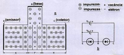 |
Principle of TRANSISTOR N-P-N considering the crystal inner strucuture.
It consists of an N-layer connected to the EMITTER (E); the P-layer
connected to the BASE (B) and finally to a second N-layer to which
the COLLECTOR (C) is connected. In the reality this arrangement
comprises two diodes in opposition with each other. (b) In the neutral
condition there is a shortage of electrons left of junction (EB),
wherea on its right there is a shortage of vancancies.
If a positive voltage with respect to (E) is applied to (B), the
potential difference will be overcome, and the diode E-B becomes
conductive in that free electrons flow toward the base in such way
this current increases with the voltage. Therefore, considering
the P-Layer has intentially been given far less dope than the N-layer,
resulting that the electrons fail to find enough vancancies to be
neutralized in the base, and will be accumulate there. If a positive
voltage with respect to (E) is applied to (C), de diode B-C will
be blocked. I.e. there will be no flow of current. If E-B is conducting,
and provided a voltage high enough, the elctrons accumulated in
B will be attracted by this external voltage. In this way a small
part of the electrons supplied by (E) will flow to (B), and a large
part will flow to (C), but the number of electons supplied by (E)
will depend on the voltage between (B) and (C). Since there is amplification,
the current toward the COLLECTOR is bigger that toward the BASE,
but itdepends on the voltage or current through the base.
|